The development of new 2D materials consisting of a layer that is one atom thick is one of the most promising areas in modern materials science. Since 2004 when the first 2D material graphene was developed scientists all over the world have been studying its characteristics.
Graphene and other 2D materials
“Interest towards graphene is only growing, - says Pavel Sorokin. – It is now entering the stage of industrial production. It least this demonstrates the huge investment made in this field by the European industry, as well as the Americans and the Chinese. Fundamental research in graphene is practically over; its qualities have been well studied. Nevertheless, huge research institutes are being set up in all those regions that will be dedicated to 2D materials focused on their application, as the knowledge of graphene qualities made the industry realize the prospects of applying 2D materials”.
“In fact, graphene was only the beginning of a huge group of 2D materials. Pretty soon it became clear that 2D materials could have a very diverse composition. Let’s take for example boron nitride or transition metal chalcogenides. Scientists all over the world are studying this family of materials. The area of studies is so large that the existing resources aren’t sufficient to cover the whole thing. But one of the most interesting and promising areas is the 2D (monolayer) materials with magnetic properties. Let me emphasize the word “monolayer” as the majority of the known quasi-monolayer materials do combine several layers, which affects their properties. Let’s take chalcogenide – it includes a layer of sulfur, a layer of metal and another layer of sulfur. Few real monolayers are known. However, those are first of all the thinnest hard substances one can imagine. And secondly, it is a macro material, in which all atoms are on the surface. If we move into the area of several layers, we immediately move into volumetric properties of materials – which is quite a different set of characteristics”.
2D material with no 3D analog
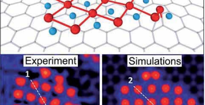
The work of scientists from the National University of Science and Technology MISiS, the Technological Institute for Superhard and Novel Carbon Materials (TISNCM), the Institute for Biochemical Physics of the RAS and their colleagues from the Japanese institute NIMS focused on the search for new 2D monolayers. The group concentrated its efforts on the opportunity of obtaining 2D materials based on metal compounds. “Earlier it was believed that compounds were unstable in 2D state and could exist exclusively as thick film with the structure similar to a bulk crystal, - Pavel Sorokin continues his story. – We showed that one could stabilize 2D structure without adding extra layers in 2D space”.
“The difficulty of finding such a structure is that a consecutive approach doesn’t work here – one cannot find the properties of a 2D material by studying a multilayer material by consecutively reducing its thickness. Such approach only more or less worked with graphene, as graphite (the predecessor of graphene) represents a multitude of loosely linked together layers of graphene. Our material does not have analogs in the 3D world. Copper oxide cannot exist as a stack of 2D sheets as they form a 3D structure with other properties. Even if we obtain two layers, they already form a cubic crystal lattice with atomic properties of a macro crystal. Already a three-layer copper oxide would possess an ordinary cubic lattice with atoms on the surface and inside. At the same time, a pure monolayer structure of copper oxide can exist only for a single sheet. That is why it is impossible to calculate the structure going from the greater to the smaller”.
The begging of the research was marked by the work published in the Science journal by scientists from China, who demonstrated that graphene’s pores could be filled with 2D metals (they used iron). “However, they didn’t understand what they had done, - Sorokin says. – It was their work that pushed me into thinking that such structures had the right to exist. And we came up with the first such material having completely defined its structure and proving in practice the accuracy of our theory”.
“Perhaps there is an element of accident in the fact that we have found such an unusual substance. On the other hand, out guess had been theoretically founded and confirmed by experiment. It is only the first work of many that will be dedicated to opening 2D structures as such structures can have a very diverse composition and fantastic properties that are simply not known yet. But it will be simpler going forward as we have already demonstrated that such a structure can exist and what properties it can have and what crystal structure it has. Now it is obvious that such structures can be created not by consecutive splitting and washing out top layers (the way graphene was obtained), but by self-assembly”. In order to develop a new substance researchers from the Japanese NIMS set copper atoms from a gas phase on partially oxidized graphene. Subsequent heating of the system forced atoms of oxygen and copper to regroup into a new structure.
According to Pavel Sorokin, graphene template-based synthesis is the only opportunity so far to obtain such 2D materials. However, taking into account technology development, such limitation can be overcome: “Currently the development of science and technology goes at such speed that what a couple of years ago was considered impossible can be done in almost any laboratory. With the help of modern technology science deals with materials at atomic level. Imagine, that one can take a stable 2D material, make a hole and place there another 2D material, which is unstable in a free state. And the stable material would prevent its unstable colleague from disintegrating. Right now it is already possible, although fairly recently it was believed that no other materials besides graphene could exist. Then it became clear that one could produce 2D structures if they were stabilized by layers of other materials, protected from oxygen influence as well as other factors, which broke down 2D structure. Then it turned out that such encapsulation (let’s say by a layer of white graphite) could stabilize structures that were unstable in principle, which in a free state were prone to self-destruction without any external influence. During the next stage multilayer hetero-structures were produced from 2D layers, which possessed absolutely new properties – the meta-materials. Now it has been demonstrated that there is a 2D structure, which does not have to be covered by a stabilizing layer. What comes tomorrow?”
New potential of the new materials
Researchers face a plethora of new opportunities for assembling other substances. Copper can form 2D structures not only with oxygen, but also with sulfur, for example. Iron, nickel, cobalt or other metals can be used instead of copper. “Currently our task is to develop the general theory for the 2D metal compounds, - says Pavel Sorokin. – Since the materials are new, it is necessary to describe everything properly, to understand, which compounds are the most interesting for us, how they can exist as the stability is essential in this case: such structure is not typical of a volumetric crystal, thus it is bound to have stability limitations”.
Despite the fundamental nature of the work, the new material has great application prospects. Researchers will have to study all the characteristics of the new material for a long time, but some things about the 2D copper oxide are already known. One of the most unusual characteristics predicted by Dmitry Kvashnin, a member of Sorokin’s team, is antiferromagnetism, which ordinary copped oxide does not demonstrate under any circumstances. Antiferromagnetic materials are considered to be very promising for microelectronics. It takes only 12 atoms of antiferromagnetic material’s surface to record one bit of information, while the existing technologies use hundreds of thousands of atoms to record one bit. “The new material can also be used for spintronics as with the addition of other materials special spin characteristics can appear at the junction. It can also be used in energy generation (to produce solar batteries). There are other possible applications – we have not studied the full spectrum of its characteristics”, - points out the researcher.
Project support
Pavel Sorokin also stressed the importance of the support for the project from the Ministry of Education and Science, as well as from the International Supervisory Board of the National University of Science and Technology MISiS: “Our infrastructure project Theoretical Materials Science of Nano Structures was set up by MISiS as a part of the program to improve the competitiveness of the leading Russian universities among the world’s top universities (Project 5-100). It is a part of the strategic academic unit “Materials and Technologies to improve the duration and quality of life”.
Our infrastructure project focused on the development of international ties between MISiS and other international research centers. We succeeded in implementing our task when we went to Japan and met with specialists from the National Institute for Material Studies (NIMS). After a set of meeting we launched onto theoretical calculations with Dmitry doing the main part. During the year and a half we managed to calculate all the characteristics, discuss all possible variants in a series of seminars and produce a world-class result together with our Japanese colleagues. The calculations were performed at the super computer cluster at the National University of Science and Technology MISiS. Without that access we would have faced a much harder task. Thus, the university has played the decisive role in creating this project. Without the university there would have been no project”.
The article about the achievements of National University of Science and Technology MISiS, the Technological Institute for Superhard and Novel Carbon Materials (TISNCM), the Institute for Biochemical Physics of the RAS and their colleagues from the Japanese institute NIMS was published in NanoScale journal.